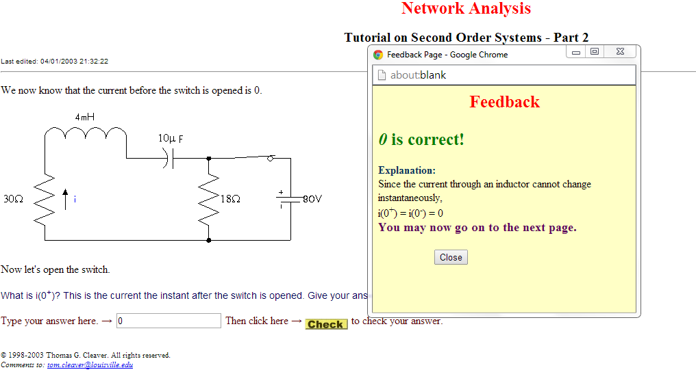
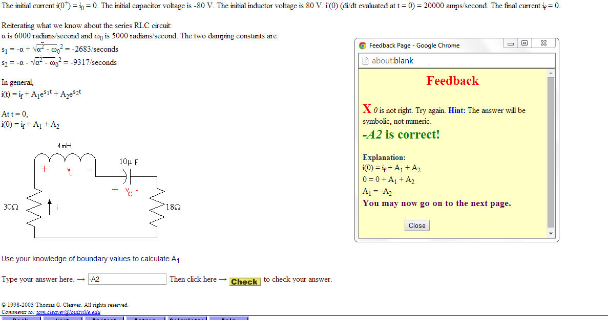
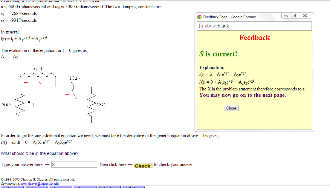
Saturday, May 24, 2014
Monday, May 12, 2014
Lab 11 - AC Circuit Capacitor
For this lab, Professor Mason hooked up a circuit into a digital oscilloscope to give a visualization of how AC voltage behaves with a capacitor.
![]() |
| Initial sine Wave |
![]() |
| Sine wave change as frequency increases |
The capacitor that was used in the circuit was about 3.4µF. The graph shows that as frequency increases, the voltage across the capacitor is decreasing.
(Note: Do not know how to do the calculation to obtain the capacitor, will add later when I figure it out. The value put is what Professor Mason set the capacitor at for the circuit)
Sunday, May 4, 2014
Lab 10 - Tutorial on Second Order Systems
The lab for this week was a tutorial on Second Order Systems:
The images below are the questions and answers (All in Order)
Total Parts: 18
Monday, April 28, 2014
Lab 9 - Capacitor Charging/Discharging
Objective:
- To test a charge/discharge system that uses a 12 V DC power supply
- Verify if the system charges within 20s with a resulting stored energy of 2.5 mJ
- Verify if the system will discharge the 2.5 mJ in 2s.
Pre-Circuit Tasks:
The circuit below shows the simple schematic of the charging/discharging system on the capacitor. To charge/discharge the capacitor, the connected to the positive side of the capacitor is placed in its respective positions. Meaning the connected cable will be attached to the CHARGE position when the capacitor is to be charged and changed to the DISCHARGE position to discharge. The rate at the which the energy is transferred is controlled by C, Rcharge, and Rdischarge.
The results for the component values:
The charging process for the capacitor was about 20 seconds.
The discharging circuit did not completely dissipate all its energy within 2 secs.
- To test a charge/discharge system that uses a 12 V DC power supply
- Verify if the system charges within 20s with a resulting stored energy of 2.5 mJ
- Verify if the system will discharge the 2.5 mJ in 2s.
Pre-Circuit Tasks:
The circuit below shows the simple schematic of the charging/discharging system on the capacitor. To charge/discharge the capacitor, the connected to the positive side of the capacitor is placed in its respective positions. Meaning the connected cable will be attached to the CHARGE position when the capacitor is to be charged and changed to the DISCHARGE position to discharge. The rate at the which the energy is transferred is controlled by C, Rcharge, and Rdischarge.
Before determining the values of the components, the expressions for the Thevenin voltage and resistance for the charging and discharging circuits were calculated.
![]() |
| Calculation for Thevenin Expressions |
Calculations for Charging/Discharging Circuit Components:
![]() |
| Charging Circuit Component |
![]() |
| Discharging Circuit Component |
C = 34.7 µF
Rcharge = 121212 Ω
Rdischarge = 12121.2 Ω
The Circuit:
![]() |
| Schematic of the Actual Circuit |
For each circuit, an oscilloscope was used to show the movement of energy within the circuit.
Charging Circuit
![]() |
| Charging Circuit |
The Vfinal obtained after 20secs was about 11.96V.
With the value of Vfinal, RLeak was determined to be 0.145 µΩ.
Discharging Circuit
![]() |
| Discharging Circuit |
Follow up Question
Practical Question:
Monday, April 21, 2014
Lab 8 - Practical Ingegrator
Sketch the input and output waveforms for 1kHz sine wave, triangle wave, and square wave inputs.
Explain the purpose of the 10 MΩ resistor's usage in the circuit
Explain the effects of removing the 10 MΩ from the circuit.
The circuit schematic below was constructed by Professor Mason.
It contains a 100k Ω resistor, a 10MΩ resistor, a 0.01µF capacitor, and an Op-Amp
The images of the wave forms are displayed on an Oscilloscope.
Red waves represent the Input waves.
Yellow waves represent the Output waves.
| Circuit Schematic (Constructed by Professor Mason) |
Red waves represent the Input waves.
Yellow waves represent the Output waves.
![]() |
| Output: Sine Wave |
In the circuit, the 10MΩ resistor is used to counter any feedback from the DC voltage. This means that if the resistor is not present within the circuit, the output waves would not be "nice" wave forms but a bunch of irregular looking waves that may contain a lot of noise and spike at random points.
Monday, April 14, 2014
Lab 7 - Practical Signal Conditioning
Objective:
Use an Op-Amp in a scaling and level-shifting circuit to change the output signal of an electronic temperature sensor to produce a temperature reading in degrees Fahrenheit.
Pre-Circuit Information/Calculations:
For the lab, the national semiconductor LM35 is used to represent the temperature in degrees Celsius. The conversion rate for the LM35 to degree Celsius is 10 mV/°C. The LM35 is tested to see if it is working properly by following the schematic below.
Once the LM35 has been tested, the following circuit is to be constructed after determining the resistors needed to satisfy the equation to convert the temperature from Celsius to Fahrenheit.
The equation to convert from Celsius to Fahrenheit:
Use an Op-Amp in a scaling and level-shifting circuit to change the output signal of an electronic temperature sensor to produce a temperature reading in degrees Fahrenheit.
Pre-Circuit Information/Calculations:
For the lab, the national semiconductor LM35 is used to represent the temperature in degrees Celsius. The conversion rate for the LM35 to degree Celsius is 10 mV/°C. The LM35 is tested to see if it is working properly by following the schematic below.
![]() |
| Schematic for to check LM35 |
![]() |
| Schematic for the Circuit |
TF = 1.8TC + 32 (Original)
TF = 1.8TC + .32 (LM35 equvialent)
The temperature conversion equation in terms of circuit elements:
VF = (1 + R2/R1)VC - R2/R1*Vref
![]() |
| Calculation for Circuit Components |
In the circuit element equation, the 1.8 from the temperature equation is represented by (1 + R2/R1). This yields the ratio value of R2/R1 which is 0.8. With the ratio obtained, the value of Vref can be determined by setting R2/R1*Vref = 0.32. This yields the value of Vref to be 0.4V. The values of R2 and R1 are determined by making sure that the ratio of the two resistors is about 0.8.
Values of Components:
Vref = 0.4 V
R1 = 2144 Ω
R2 = 1765 Ω
The Circuit:
![]() |
| The Circuit |
For the circuit, three power supplies were used. Two were set up at around 9V to power the op-amp and the LM35. The other power supply was to supply the 0.4 V for Vref. The voltmeter read about 77mV for the temperature of the room in Fahrenheit.
![]() |
| LM35 value |
The value of the LM35 was about .237 mV, which is about 24°C. Plugging this value into the Celsius to Fahrenheit conversion equation:
TF = 1.8(23.7) + 32 = 74.66 °F
The Fahrenheit temperature obtained by the voltmeter for the circuit is about 77.0 mV, which is about 77°F.
The percent error of TF:
Percent Error = (77-74.66)/ 74.66 *100 ≈ 3.13%
Subscribe to:
Posts (Atom)


